
Accueil > Équipes scientifiques > Nanophysique et Surfaces (Nanophys) > Techniques expérimentales et théoriques > Wide field optics with a scanning tunneling microscope (STM)
Wide field optics with a scanning tunneling microscope (STM)
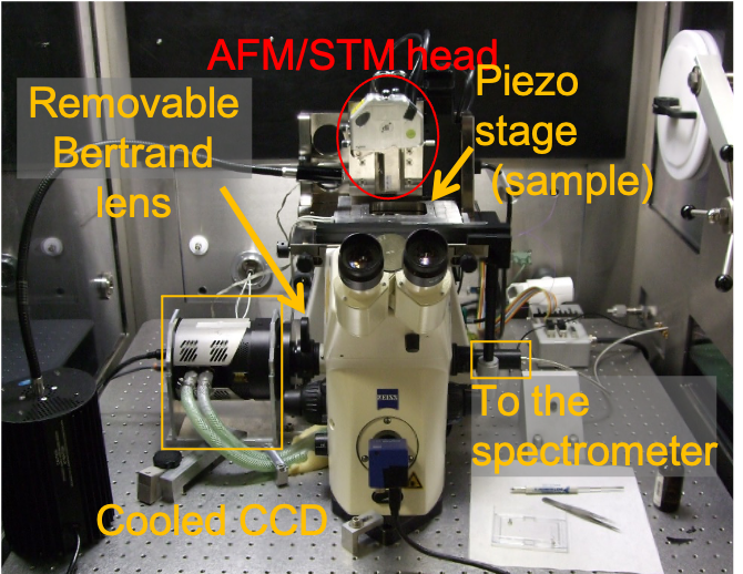
- Commercial AFM/STM head from Bruker combined with an inverse optical microscope from Zeiss
One of our novel experimental set-ups involves a commerical AFM/STM head combined with an inverted optical microscope equiped with a high-numerical-aperture objective lens (NA > 1).
In a typical experiment, the inelastic tunneling current between the STM tip and sample excites surface plasmons or excitons in the sample. These then decay radiatively and the emitted light is collected through the transparent substrate by the microscope optics. If this light is then focussed on the cooled charge-coupled device (CCD) camera, we have what we call a real plane image. From such an image we can determine from where on the sample the collected light is emitted. For instance, we can determine if the excited surface plasmons are propagating and we can study the diffusion of excitons.
We can also add an extra lens in the optical path (labeled as a Bertrand lens in the above image). In this case, the Fourier plane or back focal plane is imaged on the CCD. From this result, we can obtain at what angle the resulting light is emitted. Such information is essential for determining if the emitted light is indeed from propagating surface plasmons, and for the identification of certain physical phenomena.
The collected light may also be directed toward a spectrometer so that the energy distribution of the emitted light may be measured.
Please see the Scanning probe plasmonics and Excitonics sections for examples of how this experimental set-up may be exploited.
|
|
- Zoom sur notre STM/AFM JPK Nanowizard III et notre microscope optique Nikon
Dans la même rubrique :
- De l’optique « en plein champ » avec un microscope à effet tunnel
- Spectroscopie vibrationnelle par génération de fréquence somme (SFG)
- Le Tunnel : combiner des techniques de sciences des surfaces sous vide
- Voir des surfaces avec des atomes : “grazing incidence fast atom diffraction” (GIFAD)
- Le microscope à effet tunnel à basse température
- Outils de calcul