Leader: Eric Le Moal
Participants: Andrei Borissov, Séverine Le Moal, Elizabeth Boer-Duchemin, Gérald Dujardin
PhD students: Elysé Laurent (2023-2026), Uttam Kumar Chowdhury (visiting, 2025)
Former students: Rémi Bretel (PhD, 2018-2021), Delphine Pommier (PhD, 2017-2021), Ricardo Javier Peña Román (visiting PhD, 2021), Ala Husseen (PhD, 2015-2018)
Collaborations: Guillaume Schull and Stéphane Berciaud (IPCMS), Luiz F. Zagonel (Unicamp, Brazil), Moritz Sokolowski (Bonn, Germany), Mathieu Silly (Synchrotron SOLEIL), Andrew Mayne and Hamid Oughaddou (ISMO – SIM2D)
Contracts: ANR-22-CE09-0008 TEXTURES, ANR-16-CE24-0003 M-Exc-ICO
Motivated by the development of active optical components that can be integrated with nanoelectronics on a chip, our goal is to understand and master the emission of light from organic nanostructures and two-dimensional (2D) materials upon excitation with electrical current. The scanning tunneling microscope (STM) is used to electrically activate this luminescence within a nanoscale tunnel junction, instead of direct connections to metallic leads, in order to preserve the electronic structure of the emitters and to spatially resolve the variations of the excitation quantum efficiency.
Our activity follows three axes: (1) the nanophysics of excitons in monolayer transition metal dichalcogenides, (2) the electroluminescence of organic molecules, (3) the growth and study of model systems of thin insulating layers and organic nanostructures on these thin layers.
Techniques: STM-induced luminescence, optical spectroscopy and microscopy, STM imaging and spectroscopy, electronic spectroscopies (LEED and Auger), synchrotron-based photoemission spectroscopy
Keywords: excitons, nanooptics, transition-metal dichalcogenides (TMDs), molecular chains, alkali-halide thin films
News:
— See the synopsis “Deciphering Single-Molecule Fluorescence” in Physics Magazine (March 21, 2023), reporting on our recent paper “Many-Body Description of STM-Induced Fluorescence of Charged Molecules” (Jiang et al, Phys. Rev. Lett. 130, 126202) in collaboration with Guillaume Schull’s group.
Highlights:
The origins of electron binding energy shifts in strategic few-atom-thick insulators on metals.
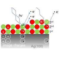
Electron binding energies and work functions are key in the electronic properties of interfaces between materials or between molecules and their substrate. These energies can be measured by photoemission spectroscopy. However, electron binding energies in presence of interfaces are subject to shifts by as much as 1 eV, because all atoms do not have equivalent dielectric environment. This issue is of paramount importance for the device industry as well as for fundamental research in physical chemistry. Theoretical modelling of the various physical effects contributing to these energy shifts is vital to prevent flawed interpretations of photoemission spectra. We provide such a modelling for ultrathin alkali-halide films on metals, which are strategic few-atom-thick insulating layers.
Article: Séverine Le Moal, Ina Krieger, Roman Kremring, Simon Weiß, Xiaosheng Yang, Serguei Soubatch, F. Stefan Tautz, Mathieu Silly, Andrei G. Borisov, Moritz Sokolowski, and Eric Le Moal, “Core-Level Binding Energy Shifts in Ultrathin Alkali-Halide Films on Metals: KCl on Ag(100)” J. Phys. Chem. C 127, 24253 (2023), pdf.
The spin and charge states an STM-excited molecule transits through before decaying.
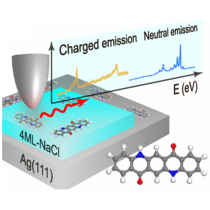
An experiment was conducted to relate the charge state of a molecule to its luminescence energy under excitation by the tunneling current of an STM. While scanning the molecule with the STM tip across different voltage ranges, sub-molecular-resolution luminescence maps of the molecule in the neutral and charged states were recorded. Based on these measurements, a model was developed to describe the spin and charge states the excited molecule transits through before radiatively decaying to the ground state. This work is a collaboration with the group of Guillaume Schull at IPCMS in Strasbourg.
Article: Song Jiang, Tomáš Neuman, Rémi Bretel, Alex Boeglin, Fabrice Scheurer, Eric Le Moal, and Guillaume Schull, “Many-Body Description of STM-Induced Fluorescence of Charged Molecules”, Phys. Rev. Lett. 130, 126202 (2023), pdf.
1D chains of dye molecules on ultrathin insulators.
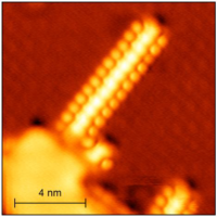
Linear chains of dye molecules on insulating thin films may become essential for the study of electronic and excitonic effects in quantum-confined molecular systems using scanning tunneling microscopy (STM). Here, we demonstrate the spontaneous growth of such linear chains via molecular self-assembly. This growth is particularly difficult due to the weak interactions between the adsorbed molecules and the insulating surface. We overcome this difficulty by using a prochiral molecule (quinacridone) and an ionic insulator (potassium chloride, KCl). We take advantage of the electrostatic interactions between the (partially charged) functional groups of quinacridone and the ions of the underlying KCl layer to stabilize the molecular chains.
Article: Rémi Bretel, Séverine Le Moal, Hamid Oughaddou, and Eric Le Moal, “Hydrogen-bonded one-dimensional molecular chains on ultrathin insulating films : Quinacridone on KCl/Cu(111)” Physical Review B 108, 125423 (2023), pdf.
Using a scanning tunneling microscope, the radiative recombination yield of excitons in a laser-excited 2D semiconductor is locally and electrically controlled.
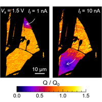
The local electrical control of the photoluminescence yield of a semiconductor is a long sought-after goal in optoelectronics, since it is the basis of future nanodevice technology. Previous attempts at such control have come up against the difficulty of controlling the local injection of charge carriers in the semiconductor and simultaneously visualizing how the diffusion and interactions of the excitons and charge carriers affect the emission properties of the semiconductor. Here, we solve this issue by exploiting the tunneling current from the tip of an STM, while simultaneously imaging the wide-field photoluminescence using an optical microscope. With this novel experimental approach, we demonstrate local, tip-induced and electrical manipulation of the excitonic photoluminescence yield in a 2D semiconductor, i.e., a tungsten disulfide monolayer (WS2).
Article: Ricardo Javier Peña Román, Rémi Bretel, Delphine Pommier, Luis E. Parra López, Etienne Lorchat, Elizabeth Boer-Duchemin, Gérald Dujardin, Andrey G. Borisov, Luiz F. Zagonel, Guillaume Schull, Stéphane Berciaud, and Eric Le Moal, “Tip-Induced and Electrical Control of the Photoluminescence Yield of Monolayer WS2” Nano Letters 22, 23, 9244-9251 (2022), pdf.
The bias polarity determines what excitons contribute to the STM-induced luminescence of 2D semiconductors.
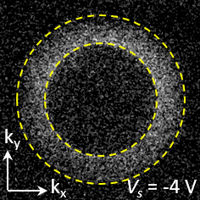
The excitonic electroluminescence of a WS2 monolayer induced by the tunneling current of an STM is measured for both (positive and negative) bias polarities of the tip-sample junction. Using optical spectroscopy and optical microscopy in Fourier space, we show that the polarity of the junction determines the spectral and angular distribution of the emitted light. As the electrons flow from the tip to the sample, the majority of the luminescence comes from charged excitons, i.e. trions.
Article: Ricardo Javier Peña Román, Delphine Pommier, Rémi Bretel, Luis E. Parra López, Etienne Lorchat, Julien Chaste, Abdelkarim Ouerghi, Séverine Le Moal, Elizabeth Boer-Duchemin, Gérald Dujardin, Andrey G. Borisov, Luiz F. Zagonel, Guillaume Schull, Stéphane Berciaud, and Eric Le Moal, “Electroluminescence of monolayer WS2 in a scanning tunneling microscope: Effect of bias polarity on spectral and angular distribution of emitted light” Phys. Rev. B 106, 085419 (2022), pdf.
STM-induced excitonic luminescence of a 2D semiconductor.
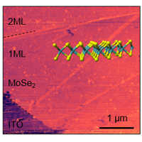
The excitons of a 2D semiconductor, i.e., monolayer molybdenum diselenide (MoSe2), are probed using an STM. Excitonic luminescence, due the radiative recombination of bright A excitons, is observed at bias voltages as low as those which correspond to the energy of the optical bandgap of monolayer MoSe2. The proposed excitation mechanism is resonance energy transfer from the tunneling current to the excitons in the semiconductor, i.e., through virtual photon coupling. Our results demonstrate a new technique for investigating the excitonic and optoelectronic properties of 2D semiconductors and their heterostructures at the nanometer scale.
Article: Delphine Pommier, Rémi Bretel, Luis E. Parra López, Florentin Fabre, Andrew Mayne, Elizabeth Boer-Duchemin, Gérald Dujardin, Guillaume Schull, Stéphane Berciaud, and Eric Le Moal, “Scanning tunneling microscope-induced excitonic luminescence of a two-dimensional semiconductor” Phys. Rev. Lett. 123, 027402 (2019), pdf, suppl. material.
Electron induced reactions of NaCl on Silver.
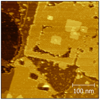
Alkali halides, e.g., NaCl, are ideal materials with wide electronic band gaps that can be grown in thin films. These thin films can then act as spacers to electronically decouple organic molecules from a metal substrate so that the molecules retain their intrinsic electronic and optical properties. We studied the structure and stability of NaCl thin films grown on the Ag(001) substrate, using a multi-technique approach with STM and STS, LEED, and Auger electron spectroscopy (AES).
Article: A. Husseen, S. Le Moal, H. Oughaddou, G. Dujardin, A. Mayne, and E. Le Moal, “Reaction kinetics of ultrathin NaCl films on Ag(001) upon electron irradiation”, Phys. Rev. B 96, 235418 (2017), pdf.
