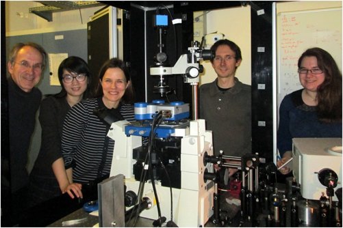
Leader: Elizabeth Boer-Duchemin
Participants: Eric Le Moal, Andrei Borissov, Gérald Dujardin, Georges Raseev
Postdocs: Aakansha Suchitta, Pavel Varlamov
PhD student: Elham Fakhrzadeh
Past contributors: Geneviève Comtet (DR), Yang Zhang (Post-doc), Damien Canneson (Post-doc), Tao Wang (PhD), Benoit Rogez (PhD), Shuiyan Cao (PhD), Moustafa Achlan (PhD), Delphine Pommier (PhD), Jean-François Bryche (Post-doc), Zélie Hufschmitt (PhD)
Our goal is to realize and exploit electrical nanosources of photons and plasmons. Towards this aim, we have developed an experimental apparatus consisting of a scanning tunneling microscope (STM) coupled to an inverse optical microscope. The inelastic tunnel current of the STM may electrically and locally excite surface plasmons on the metal nanostructured sample. The resulting emission is collected by the microscope objective.
Techniques: STM – AFM – Optical microscopy and spectroscopy
News
— The Paris-Saclay Plasmonics School (PS)²2025, the third edition of a biennial thematic school organized by the Institute for the Sciences of Light at Paris-Saclay University, will take place on July 7-11, 2025 in Orsay (France). The school aims to provide a comprehensive introduction to the field of plasmonics, offering participants the chance to engage with leading experts and explore cutting-edge research in this rapidly evolving discipline. As with previous editions, we encourage early-career graduate researchers—including Master’s and Ph.D. students, postdocs, and junior faculty—to apply!
Highlights:
Can the plasmon resonance of a nanoparticle be measured using a scanning probe microscope?
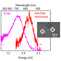
The optical response of single plasmonic nanoparticles measured under inelastic-tunneling excitation in an STM is shifted and broadened as compared to what is obtained from light scattering in a dark-field optical microscope. Based on numerical simulations using the finite-element method, we show that the near-field excitation, the effect of the tip and the additional screening effect due to the water bridge in the STM-based experiments carried out under ambient conditions each contribute a significant part to the these spectral shift and peak broadening. Our results are true in virtually any optical measurement using a scanning probe microscope operated in air.
Article : Mario Zapata-Herrera, Benoît Rogez, Sylvie Marguet, Gérald Dujardin, Elizabeth Boer-Duchemin, and Eric Le Moal, “Spectral shifts in tip-induced light from plasmonic nanoparticles in air”, Phys. Rev. B 109, 155433 (2024), pdf
A new way to interrogate single tunnel-junction nanoantennas.
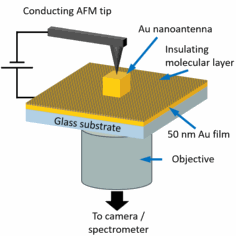
An essential component of integrated plasmonic circuits is an electrical nanoscale source of surface plasmon polaritons. We demonstrate that such a source can be obtained by using the tunneling junction formed between a plasmonic nanoantenna (a chemically-synthesized gold nanocube) and a thin gold film, separated from each other by an insulating molecular layer. A potential difference must be applied between the nanoantenna and film, so that the inelastic tunneling current in the junction may excite propagating surface plasmons on the Au layer. To do this we have developed an original method using the biased conducting tip of an atomic force microscope to temporarily complete the circuit on the nanoscale while performing sensitive optical measurements. The advantages of this method include that (1) different nanoantenna junctions may be rapidly tested without the need of bulky contacts made by lithography and (2) the excitation is restricted to the junction, as would be the case in a real device.
Article : D. Pommier, Z. Hufschmitt, C. Zhang, Y. Lai, G. Dujardin, E. Le Moal, C. Sauvan, J.-J. Greffet, Jianfang Wang, and Elizabeth Boer-Duchemin, “Nanoscale Electrical Excitation of Surface Plasmon Polaritons with a Nanoantenna Tunneling Junction”, ACS Photonics 10(8), 2641–2649 (2023), pdf
A new probe of the photonic LDOS.
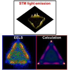
While the scanning tunneling microscope (STM) is a well-known tool for the investigation of the local electronic density of states (e-LDOS), can it also be used to study the electromagnetic local density of states (EM-LDOS)? To answer this question, we use the STM to locally excite the plasmonic modes of a gold triangular platelet. We then measure the spectra and energy-filtered images of the radiative decay of these modes. By comparing our results to electron energy loss spectroscopy (EELS) measurements on similar nanoparticles and to calculations, we show that the light emitted from the STM-nanosource is indeed related to the radiative contribution of the EM-LDOS. Thus, the scanning tunneling microscope offers an extremely attractive method to locally, and eventually simultaneously, probe the atomic, electronic, and photonic structure of a nano-object.
Article : S. Cao, M. Zapata-Herrera, A. Campos, E. Le Moal, S. Marguet, G. Dujardin, M. Kociak, J. Aizpurua, A. G. Borisov, and E. Boer-Duchemin, “Probing the Radiative Electromagnetic Local Density of States in Nanostructures with a Scanning Tunneling Microscope”, ACS Photonics 7 (5), 1280–1289 (2020), pdf
Optical mode’s dispersion relation at a glance.
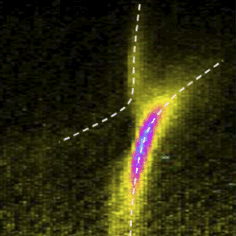
A new single-image acquisition technique for the determination of the dispersion relation of the optical modes of a plasmonic multilayer stack is introduced. The optical modes are electrically excited using the STM tip and their energy-momentum dispersion relation is determined from the angle-resolved optical spectrum of the resulting light.
Article : S. Cao, M. Achlan, J.-F. Bryche, Ph. Gogol, G. Dujardin, G. Raşeev, E. Le Moal, and E. Boer-Duchemin, “An electrically induced probe of the modes of a plasmonic multilayer stack”, Opt. Express 27 (23), 33011-33026 (2019)
Electrical light beams on design.

A very simple and broadband optical antenna, consisting of a single elliptical slit etched in a gold film, is used to electrically generate light beams in controlled directions, which are determined by the eccentricity of the ellipse.
Article : S. Cao, E. Le Moal, Q. Jiang, A. Drezet, S. Huant, J.-P. Hugonin, G. Dujardin, and E. Boer-Duchemin, “Directional light beams by design from electrically driven elliptical slit antennas”, Beilstein J. Nanotechnol. 9, 2361-2371 (2018), pdf
k-space optical microscopy, revisited.
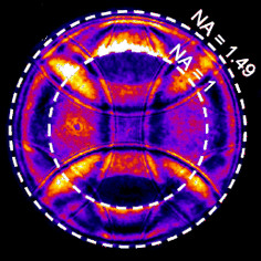
An exhaustive study of the effects and artefacts by which the image is formed in optical microscopy of the Fourier plane, on periodic samples. These artifacts, used to exceed the diffraction limit, can be exploited for nano-positioning and autofocus applications in light microscopy.
Article : J.-F. Bryche, G. Barbillon, B. Bartenlian, G. Dujardin, E. Boer-Duchemin, and E. Le Moal, “k-space optical microscopy of nanoparticle arrays : Opportunities and artifacts”, J. Appl. Phys. 124, 043102 (2018), chroniqué sur le site Scilight, pdf, suppl. mat.
Make plasmonic lenses resonate!
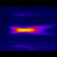
The unique combination of scanning tunneling microscopy (STM) and angle-resolved optical spectroscopy is used to probe the spectral response of a plasmonic lens. Simple design rules for optimized light beaming from plasmonic lenses with the smallest possible footprint are proposed, in the view of their integration with electronics into devices.
Article : S. Cao, E. Le Moal, F. Bigourdan, J.-P. Hugonin, J.-J. Greffet, A. Drezet, S. Huant, G. Dujardin, and E. Boer-Duchemin, “Revealing the spectral response of a plasmonic lens using low-energy electrons”, Phys. Rev. B 96, 115419 (2017), pdf, suppl. mat.
SPP beams from plasmonic crystals.
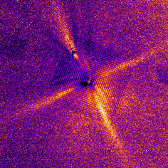
Surface plasmon polariton (SPP) beams with an in-plane angular spread of 8° are produced by electrically exciting a 2D plasmonic crystal using a scanning tunneling microscope (STM). The plasmonic crystal consists of a gold nanoparticle (NP) array on a thin gold film on a glass substrate and the inelastic tunnel electrons from the STM provides a localized and spectrally broadband SPP source. Surface waves on the gold film are shown to be essential for the coupling of the local, electrical excitation to the extended NP array, thus leading to the creation of SPP beams.
Article : D. Canneson, E. Le Moal, S. Cao, X. Quélin, H. Dallaporta, G. Dujardin, and E. Boer-Duchemin, “Surface plasmon polariton beams from an electrically excited plasmonic crystal”, Opt. Express 24(23), 26186-26200 (2016)
Tip instability matters for STM-induced light in air.
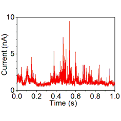
We demonstrate that the optimum mode of operation of the STM for maximum photon emission is completely different in air than in vacuum. To this end, we investigate the emission of photons, the variation in the relative tip-sample distance and the measured current as a function of time for an STM operating in air. The current instabilities are shown to be a key ingredient for producing intense light emission from an STM operating in ambient conditions (photon emission rate several orders of magnitude higher than for stable current). These results are explained in terms of the interplay between the tunnel current and the electrochemical current in the ubiquitous thin water layer that exists when working in air.
Article : B. Rogez, S. Cao, G. Dujardin, G. Comtet, E. Le Moal, A. Mayne, and E. Boer-Duchemin, “The mechanism of light emission from a scanning tunnelling microscope operating in air”, Nanotechnology 27(46), 465201 (2016)
How to control STM-induced light using a gold nanoparticle.
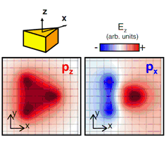
The properties of STM-induced light are difficult to control because of the strong influence of the STM tip. In this work, we show both theoretically and experimentally that the sought-after, well-controlled emission of light from an STM tunnel junction may be achieved using a nonplasmonic STM tip and a plasmonic nanoparticle on a transparent substrate. We demonstrate that the native plasmon modes of the nanoparticle may be used to engineer the light emitted in the substrate.
Article : E. Le Moal, S. Marguet, D. Canneson, B. Rogez, E. Boer-Duchemin, G. Dujardin, T. V. Teperik, D.-C. Marinica, and A. G. Borisov, “Engineering the emission of light from a scanning tunneling microscope using the plasmonic modes of a nanoparticle”, Phys. Rev. B 93, 035418 (2016), pdf
STM excitation of photonic–plasmonic hybrid systems.
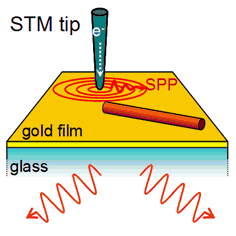
We report on the optical and electrical excitation of the modes of a “hybrid” waveguide consisting of a single organic nanofiber on a thin gold film. Two guided modes of mixed photonic–plasmonic character are identified and the dispersion relations of this hybrid waveguide are determined. A local electrical nanosource of surface plasmon polaritons (SPPs) is coupled to the hybrid waveguide. We show that the electrically excited SPPs couple to the fundamental mode and that the coupling efficiency is highest when the SPP nanosource is aligned with the nanofiber axis.
Article : B. Rogez, R. Horeis, E. Le Moal, J. Christoffers, K. Al-Shamery, G. Dujardin, and E. Boer-Duchemin, “Optical and Electrical Excitation of Hybrid Guided Modes in an Organic Nanofiber–Gold Film System”, J. Phys. Chem. C 119 (38), 22217–22224 (2015)
Scattering at gold nanoparticles reveals the mutual coherence of STM-excited light and SPPs.
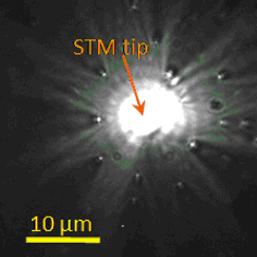
We study the scattering of electrically excited surface plasmon polaritons (SPPs) from gold nanoparticles (NPs) on a thin gold film. Interaction of the excited SPPs with the NPs leads to both in-plane (SPP-to-SPP) and out-of-plane (SPP-to-photon) scattering. We use SPP leakage radiation microscopy to monitor the interference between the incident and in-plane scattered SPP waves. As well, the out-of-plane scattered radiation interferes with the direct light emission from the STM tip in the Fourier plane. This confirms the mutual coherence of the light and SPP emission resulting from the inelastic tunneling of an electron in the STM junction.
Article : T. Wang, B. Rogez, G. Comtet, E. Le Moal, W. Abidi, H. Remita, G. Dujardin, and E. Boer-Duchemin, “Scattering of electrically excited surface plasmon polaritons by gold nanoparticles studied by optical interferometry with a scanning tunneling microscope”, Phys. Rev. B 92, 045438 (2015), pdf
The temporal coherence of STM-excited SPPs.
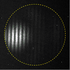
The temporal coherence of propagating surface plasmons is investigated using a local, broadband plasmon source consisting of an STM. A variant of Young’s experiment is performed using a sample consisting of a 200-nm-thick gold film perforated by two 1-μm-diameter holes (separated by 4 or 6 μm).
Article : T. Wang, G. Comtet, E. Le Moal, G. Dujardin, A. Drezet, S. Huant, and E. Boer-Duchemin, “Temporal coherence of propagating surface plasmons”, Opt. Lett. 39, 6679 (2014)
A Young’s experiment for plasmons and the spatial coherence of STM-excited SPPs.
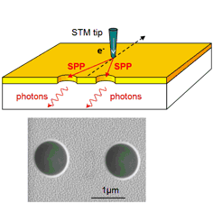
An SPP-Young’s experiment is performed, where an STM-excited SPP wave is incident on a pair of 1 μm diameter holes in a thick gold film on a glass substrate. The visibility of the resulting fringes in the Fourier plane is analyzed to show that the polarization of the electric field is maintained when SPPs scatter into photons. From this SPP-Young’s experiment, an upper bound of ≈200 nm for the radius of this STM-excited source of surface plasmon polaritons is determined.
Article : T. Wang, E. Boer-Duchemin, G. Comtet, E. Le Moal, G. Dujardin, A. Drezet, and S. Huant, “Plasmon scattering from holes : from single hole scattering to Young’s experiment”, Nanotechnology 25(12), 125202 (2014), arXiv : 1401.2002
An electrical, radially polarized, micro-sized light beam.
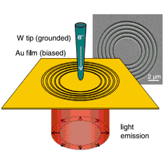
Cylindrical vector beams are produced from a low-energy, electric, microscale light source, by combining a “plasmonic lens” with the ability to locally and electrically excite propagating surface plasmons on gold films from the inelastic tunneling of electrons. We report on the emission of radially polarized beams with an angular divergence of less than 4°.
Article : S. Cao, E. Le Moal, E. Boer-Duchemin, G. Dujardin, A. Drezet, S. Huant, “Cylindrical vector beams of light from an electrically excited plasmonic lens”, Appl. Phys. Lett. 105, 111103 (2014), pdf ; acte de conférence : S. Cao, M. Lequeux, E. Le Moal, A. Drezet, S. Huant, G. Dujardin, E. Boer-Duchemin, “Using a plasmonic lens to control the emission of electrically excited light”, Proc. SPIE 9884, Nanophotonics VI, pp.98841Y (2016), pdf
Graphene makes QDs blink less and emit faster.
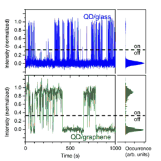
A new class of optoelectronic nanodevices consisting of 0D semiconductor nanocrystals and 2D single graphene layers may be used to investigate and control the transfer of energy and charge in low-dimensional systems. Here, we investigate the fluorescence dynamics of individual colloidal quantum dots (QDs) on graphene on both the nanosecond time scale (fluorescence lifetime) and the 1−100 s time scale (blinking statistics).
Article : B. Rogez, H. Yang, E. Le Moal, S. Lévêque-Fort, E. Boer-Duchemin, F. Yao, Y.-H. Lee, Y. Zhang, D. Wegner, N. Hildebrandt, A. Mayne, G. Dujardin, “Fluorescence lifetime and blinking of individual semiconductor nanocrystals on graphene”, J. Phys. Chem. C 118, 18445 (2014), pdf
Directional light from an electrical nanosource.
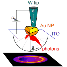
We report on the local, low-energy, electrical excitation of localized surface plasmons (LSP) on individual gold nanoparticles (NPs) using an STM. Selective excitation of the out-of-plane and in-plane dipolar LSP modes of the NP is achieved through the lateral position of the tip with respect to the symmetry center of the NP. This allows controlling the angular distribution, polarization, and spectrum of the resulting emission of light.
Article : E. Le Moal, S. Marguet, B. Rogez, S. Mukherjee, P. Dos Santos, E. Boer-Duchemin, G. Comtet, G. Dujardin, “An electrically excited nanoscale light source with active angular control of the emitted light”, Nano Lett. 13, 4198 (2013), pdf
Edge scattering reveals STM-excited SPPs on the top and bottom sides of a gold stripe.
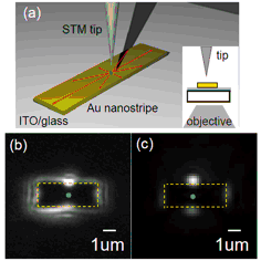
The scattering of electrically excited surface plasmon polaritons (SPPs) into photons at the edges of gold metal stripes is investigated. SPPs propagating on the air-gold interface scatter at the stripe edges into light emitted in the forward direction and at large angle (close to the air-glass critical angle). SPPs on the gold-substrate interface yield a weaker isotropic component of the scattered light, which forms an interference pattern in the Fourier plane images.
Article : Y. Zhang, E. Boer-Duchemin, T. Wang, B. Rogez, G. Comtet, E. Le Moal, G. Dujardin, A. Hohenau, C. Gruber, and J. R. Krenn, “Edge scattering of surface plasmons excited by scanning tunneling microscopy”, Opt. Express 21(12), 13938 (2013)
The STM excites localized and propagating surface plasmons.
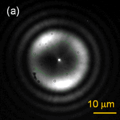
We have demonstrated the local, electrical excitation of propagating surface plasmons on thin gold films using the STM. This excitation process relies on inelastic tunneling effects. Its confinement to the tunnel junction between tip and surface provides unmatched spatial resolution that is far beyond the possibilities of optical excitation.
Article : T. Wang, E. Boer-Duchemin, Y. Zhang, G. Comtet and G. Dujardin, “Excitation of propagating surface plasmons with a scanning tunnelling microscope”, Nanotechnology 22, 175201 (2011)
