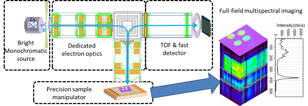
The HREELM project is the built of the first working prototype of a high resolution electron energy loss microscope (HREELM) to study nanoscale, surface vibrational order. The instrument will be able to do full field imaging of low energy electron energy losses (in real and in reciprocal space) by combining nanometric spatial (20 nm) and high spectral resolution (10 meV, 80 cm-1). It will allow for the first time mapping of vibrational states over microscopic, heterogeneous regions of a sample surface, on the scale of natural and artificial structures such as grains, domains, circuits and functional patterning.
The HREELM is developped in a close collaboration between the institut (ISMO), the Laboratoire Aimé Cotton, and the IRAMIS du CEA.

Many surface science challenges require a thorough understanding of the chemical nature of surfaces and interfaces, where couplings occur between excited states resulting from radiation absorption and pathways to utilization or losses. Imaging of surface vibration will help identify the chemical nature of surfaces and their coupling to vibration.
The instrumental challenge of HREELM is to combine monochromatic low energy electrons with high spectroscopic, spatial and wave number resolution.
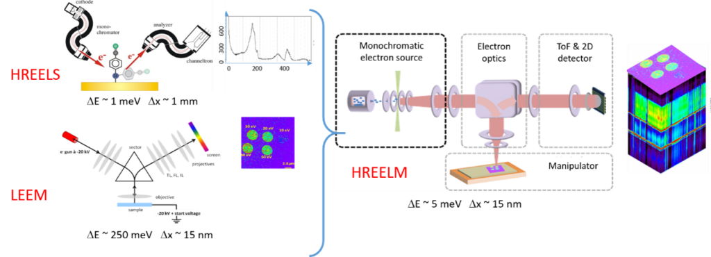
In a nut shell, the instrument concept consists of coupling the performances of two surface sensitive instruments, hitherto mutually exclusive, working in the low energy electron interaction regime: on the one hand, the spectral analysis capability of the HREELS (High-Resolution Electron Energy Loss Spectroscopy), on the other hand, the spatial resolution of LEEM (Low Energy Electron Microscopy). The combination of the two is only made possible by the unique technological innovations inherent in our HREELM conception. This patented concept is based on the use of an innovative electron source (highly monochromatic), available in our consortium and new low energy electron optics, specially designed to preserve the spectral resolution.

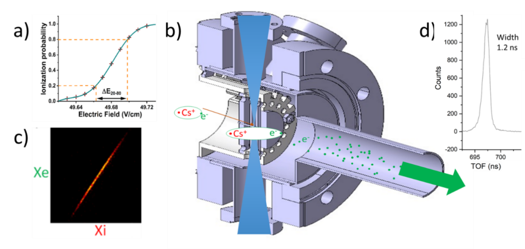
Resolving vibrational structure relies on a narrow bandwidth (in the few meV range) electron source. Conventional electron sources (tungsten filaments, LaB6 crystals or field emission guns) have, at best, ~ 250 meV energy resolution. The narrow band pass can be achieved by use of a monochromator as in HREELS, but this attenuates the beam current and increases angular divergence, making high resolution imaging impossible. We use a completely new source based on laser-induced-ionization of an atomic beam emitted from an effusive oven to provide an intrinsically monochromatic electron beam. Such threshold photo-ionization electron sources can produce monochromatic beams with energy width below 2 meV and have mainly been used in laboratories to study collisions between electrons and atoms or molecules but, as yet have not been used for microscopy. There are several reasons for this, including current limitations (typically 100 pA, whereas 1 nA is usually required to acquire an image in a reasonable time), the need for intense (several watts) continuous laser to photo-ionize the atoms.


coming soon….
Coming soon …..